

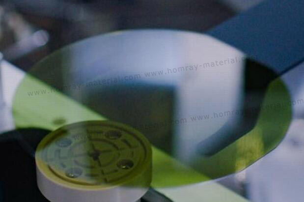
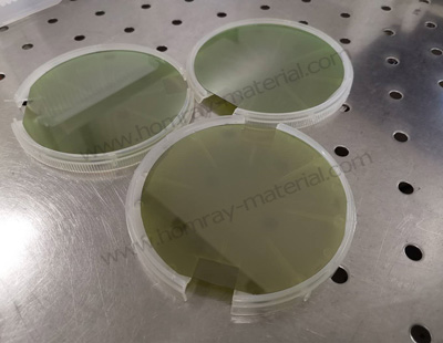
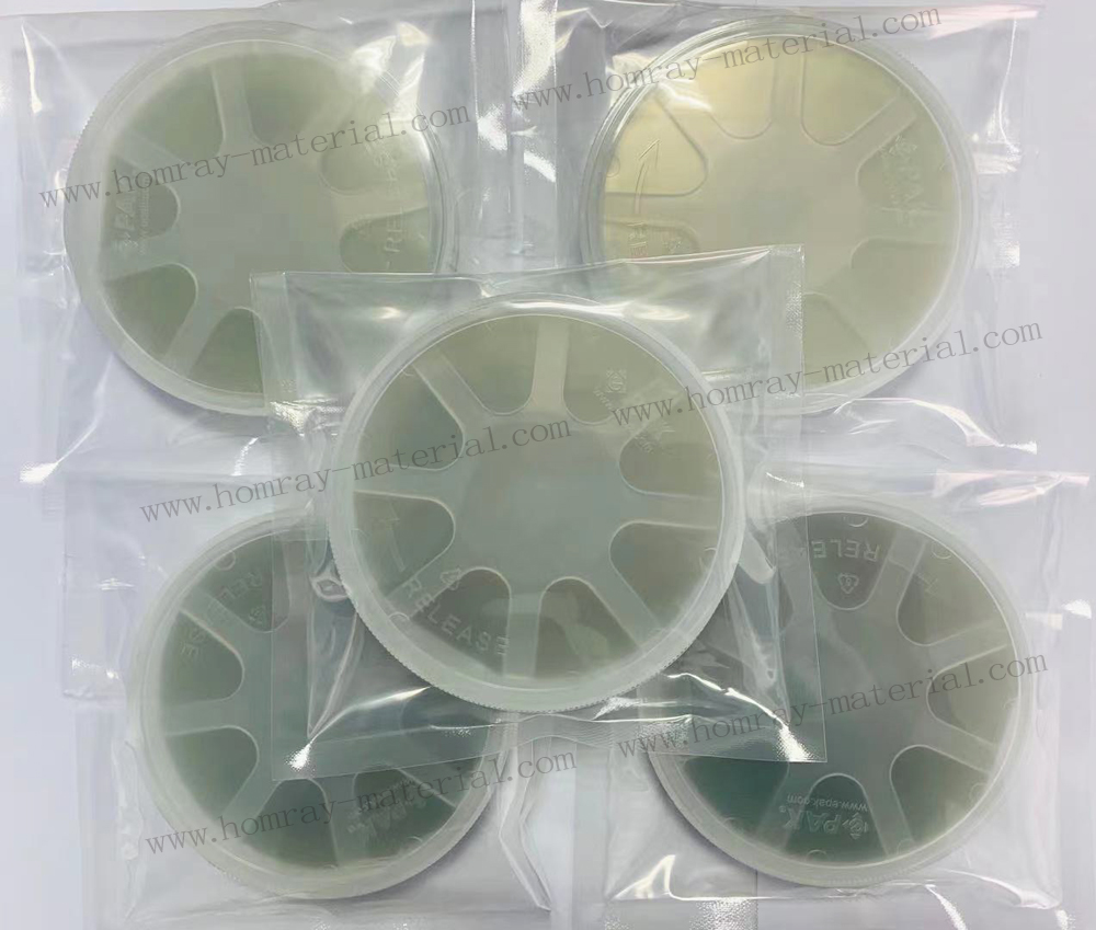
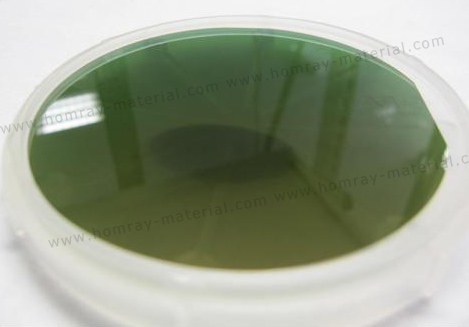
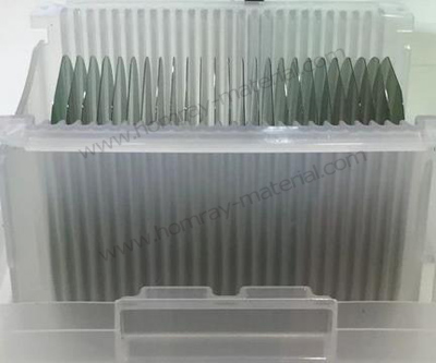
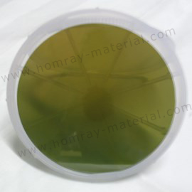
4inch 4H-N SiC Substrate Wafer
Silicon Carbide (SiC) Substrate
Diameter: 100±0.5mm
Thickness:350±25um
Doping : Nitrogen
Product Description
As the leading manufacturer and supplier of SiC (Silicon carbide) substrate wafer, Homray Material Technology can provide 4 inch Production Grade of 4H-N SiC Substrate. Silicon carbide (SiC)subsrate wafer is the next generation semiconductor material, with unique electrical
We also provide Dummy Grade SiC substrate and Research Grade SiC wafer. Meanwhile, the best grade in HMT is ultralow MPD Grade with favourable price.
Below is the brief spec, please contact us for detailed PDF spcification with email or mobile phone.
- Diameter: 100±0.5 mm
- Thickness:350 μm±25μm
- Orientation:Off axis : 4.0° toward < 1120>±0.15°
- Resistivity:0.015~0.025 Ω·cm
- Double Side Polished
SiC material wide energy Gap (Band Gap) than the existing Si (silicon) Gap width more than 3 times wider, can withstand more than 10 times the voltage, SiC low loss, high power characteristics suitable for high voltage and high current application field, including electric vehicles, electric vehicle charging infrastructure, solar energy and offshore wind power and other green power generation equipment.ompared with traditional Si, the third-generation semiconductor material SiC can reduce the power conversion loss by 50%, reduce the power conversion cost by 20%, and improve the endurance of electric vehicles by 4%.
Related Products
 Homray Material Technology. All rights Reserved.
![]() E-mail:kim@homray-material.com;tina@homray-material.com
E-mail:kim@homray-material.com;tina@homray-material.com
![]() M.P: +86-15366208370 ; +86-15366203573
M.P: +86-15366208370 ; +86-15366203573
Gallium Nitride (GaN) Substrate Website: www.gansubstrate-hmt.com